3 Bit Flash Adc Pdf
Digitizer includes a 3-bit Analog-to-Digital Converter ADC and three demultiplexers DEMUX in Fig1 one for each ADC output bit. Journal of Computer Applications 0975-8887 vol.
Pdf A 3 Bit 10 Msps Low Power Cmos Flash Adc
A threshold block to generate a plurality of thresholds wherein each of said thresholds represents a different strength in a strength range of interest.

. The right balance of CTLE circuitry and flash ADC sizes and number play a key role in minimizing ADC bits to achieve minimum area and power. 16 or 32 KB Flash 5 timers ADC and 4 communication interfaces Datasheet -production data Features Core. As shown in figure 2.
Now all the outputs of the comparator becomes inputs of the encoder it means that the input of the priority encoder depends on the output of comparator and the Encoder gives the digital output of input when two or more than two inputs are high at the same time it produces the binary code of the input which has Highest Priority. The design of a state-of-the-art 112-gigabits-per-second. 3-bit All-Parallel Flash Converter.
Our Services Order Now Discounts. New power saving design method for CMOS flash ADC. Published 24 August 2017.
As the analog input voltage exceeds the reference voltage at each comparator the comparator outputs will sequentially saturate to a high state. In addition the individual comparators provide. The proposed architecture can be extended to higher resolution.
The following illustration shows a 3. The sampling function which is necessary. The block diagram of Figure 5 shows a multi-bit Σ-Δ ADC which uses an n-bit flash ADC and an n-bit DAC.
Thus conversion time is very short for example for 12-bit ADC with clock frequency of 1MHz the conversion time will be 121µs12µs only. At the output of the comparators the sampled input. Aug 24 2017 The Flash ADC A Circuit for All Seasons B.
A 3-Bit Pseudo Flash ADC Based Low-Power CMOS Interface Circuit Design for Optical Sensor. IEEE Transactions on Circuits and Systems vol. Also flash ADCs are too costly for high resolutions because their complexity increases exponentially with the number of bits.
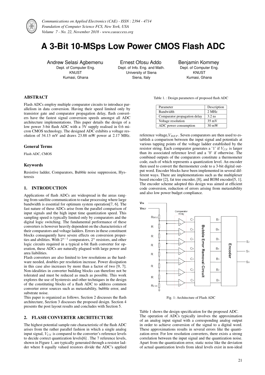
Literature review Thesis Revision Interview Literary analysis Multiple Choice Questions Outline Dissertation PDF Poster Dissertation chapter - Abstract Reaction paper Thesisdissertation chapter Thesis Proposal Dissertation chapter. A flash analog to digital converter ADC to generate digital codes representing a strength of an input signal at a sequence of time instances said flash ADC comprising. Shown in Figure 1 an N-bit flash ADC employs 2N com-parators along with a resistor ladder consisting of 2N equal segments.
The ADC sampling frequency is 4 GHz and the DEMUX stage decreases the data flow down to 250 MHz before the data are further processed transported through an optic fiber line and finally correlated. Different type of ADCs are available like SAR ADC Dual Slope ADC Sigma Delta ADC and Flash ADC but among all the se the most commonly used ADC is The Flash adc because of its better tradeoff between its performance metrics. Leakage current mechanisms and leakage reduction techniques in deep-submicron CMOS circuits.
ADC 3-bits Flash I- Introduction We have decided to design an one-step Flash converter. 3 Bit Flash Adc Thesis Report Pdf - 475. As shown in the schematic below in this type of ADC the input signal is compared to the 2ⁿ nodes of resistors.
3-bit and 4-bit Flash ADC respectively. The following illustration shows a 3-bit flash ADC circuit. To convert an analog signal to digital form we can compare its value against a number of equally spaced reference voltages that span the expected range of input amplitudes.
10-bit ADC 3 timers UART SPI I2C Datasheet -preliminary data Features Core 16 MHz advanced STM8 core with Harvard architecture and 3-stage pipeline Extended instruction set Memories Program memory. V ref is a stable reference voltage provided by a precision voltage regulator as part of the converter circuit not shown in the schematic. The circuit operates with an input frequency of 25MHz and 15V supply with a conversion time of 2162ns and 6182ns for 3-bit and 4-bit ADC respectively.
What is claimed is. Up to 24 cash back If VIN is greater than Vref the output is 1 otherwise 0. RESULTS The 3-bit ADC based on flash type is designed in standard.
The method used for 3 Bit Flash ADC demonstate the use of Low power Comparator in Flash ADC. Design and implementation of 4-bit flash ADC using folding technique in cadence tool. Final output of 3bit Flash ADC Figure 11 shows the output of final 3-bit flash ADC designed.
For this reason the flash ADC is capable of high speed. The input signal is applied to all the comparators at once so the thermometer output is delayed by only one comparator delay from the input and the encoder N-bit output by only a few gate delays on top of that so the process is very fast. The ADC design can be used for low power and high speed applications.
A 3-bit Flash ADC has been designed using CMOS technology. 1Block diagram for 3-bit Flash ADC Flash analog-to-digital converters also known as parallel ADCs are the fastest way to convert an analog signal to a digital signal. Full PDF Package Download Full PDF Package.
Amc1200 Neizolirovannyj Istochnik Pitaniya Dlya Amc1200 Amc1301 Forum Amplifiers Usiliteli Soobshestvo Ti E2e Power Power Supply Logic

Three Bit Flash Adc Transient Response For A Frequency Of 10 Mhz The Download Scientific Diagram

Nodemcu Esp8266 Pinout With Detailed Board Layout Analog To Digital Converter Development Board Microcontrollers

Pin Diagram Of Cf Compact Flash Memory Card Teknoloji


Comments
Post a Comment